
The Chip Only Three Companies Can Build: The Full Research Note
The complete case, section by section: the economics that created the bottleneck, the company that started it, the machine that makes it possible, the AI boom straining it to breaking point, and the geopolitics now riding on all of it.
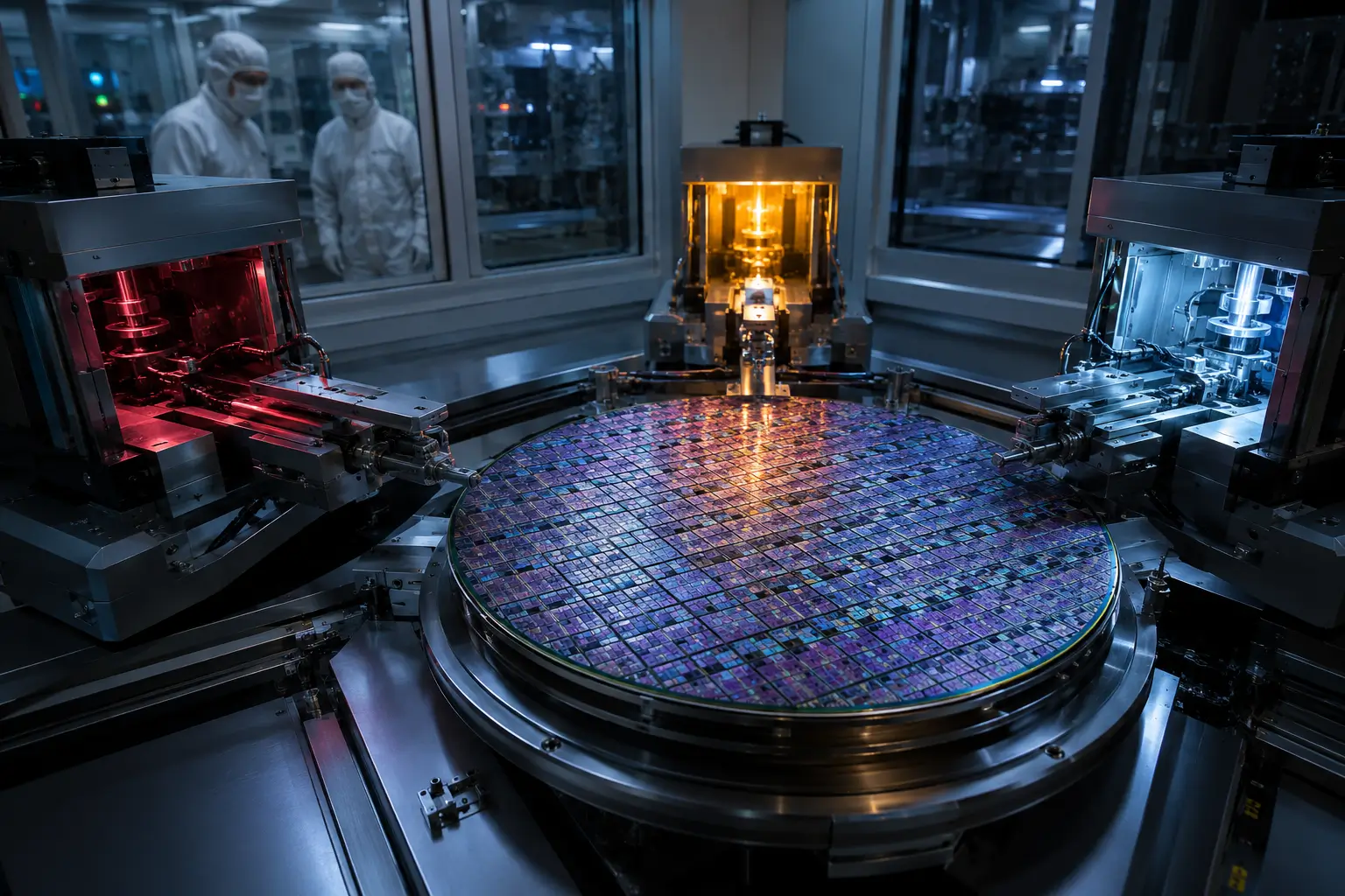
Somewhere in the Netherlands, a machine the size of a city bus fires molten tin with a laser fifty thousand times a second, producing light hotter than the surface of the sun. Only one company on earth knows how to build that machine — and without it, nothing described in the rest of this piece would be possible.
Every smartphone, AI server, electric vehicle, and modern weapons system depends on advanced semiconductors — logic chips manufactured at the very edge of what physics currently allows. Making them is one of the hardest industrial feats humans have ever attempted, and the difficulty has produced an extraordinary bottleneck: almost the entire world’s supply of leading-edge chips passes through one company, on one island, using machines built by one other company. This note walks through how that happened, section by section, with the numbers behind each part of the story.
01 — Market StructureThe Concentration
Ask which companies can actually manufacture a modern leading-edge chip — the kind inside an iPhone, an Nvidia GPU, or a fighter jet’s radar system — and the honest answer is: almost none of them. Taiwan Semiconductor Manufacturing Company, known as TSMC, now produces roughly 90% of the world’s chips built at 5 nanometers or smaller, the class of manufacturing that defines the current frontier. By 2026 the company’s market capitalization had crossed $2 trillion, and its revenue for 2025 alone topped $122 billion, with a net profit margin above 45%.

Samsung, in South Korea, holds most of what’s left, though it has struggled with lower yields — the percentage of usable chips produced per wafer — at its most advanced nodes. Intel, once the industry’s defining name, barely registers at the leading edge. The company that essentially invented the modern chip industry has spent much of the last decade falling behind its own manufacturing roadmap, missing self-imposed deadlines for years in a row. The slide became serious enough that the US government took a 10% equity stake in Intel in August 2025 — an extraordinary intervention for a company that once symbolized American industrial dominance.
This concentration is not the result of a lack of competitors trying. Twenty-five years ago, roughly forty companies worldwide could plausibly build a leading-edge fab. Today there are effectively three, and only one of them is reliably shipping at the true frontier. Understanding why requires understanding the economics in the next section — because the story of the chip industry, more than almost any other, is a story about a cost curve that simply outran nearly everyone’s ability to keep climbing it.
02 — EconomicsThe Cost of Staying in the Game
Semiconductor engineers have long lived by two laws, one famous and one not. The first, Moore’s Law, is well known: the number of transistors that can be packed onto a chip roughly doubles every two years, driving relentless gains in performance. The second, coined by venture capitalist Arthur Rock and known as Rock’s Law, gets far less attention but arguably matters more for understanding market structure: the cost of building a factory capable of keeping pace with Moore’s Law roughly doubles every four years.
In the early 1970s, a semiconductor fab cost on the order of a few million dollars, about $30 million in today’s money. By the late 1990s that figure had reached roughly $2 billion. By 2009, around $4 billion. TSMC’s Arizona fab, announced in 2019, was projected at $12 billion. Today, a single leading-edge facility can run $28 billion or more — a nearly thousandfold increase since the 1970s, even after adjusting for inflation.
Economic research backs up the scale of that slowdown from the other direction. The classic two-to-three-year cadence between new manufacturing “nodes” — the cycle that produced Moore’s Law’s steady 20–30% annual decline in the cost of a transistor — effectively broke in 2014, when the jump to the next node stretched to roughly four years. US government price data on microprocessors tell the same story: prices that fell by nearly half each year through the late 1990s and early 2000s were declining by only about 3% a year between 2011 and 2015. Part of the reason is the photomask, the physical stencil used to print each chip layer: a set that cost $450,000 to $700,000 at the 130-nanometer node in the early 2000s costs $10 million to $18 million today — a 20-to-40-fold jump that has to be earned back before a single chip is profitable.

That exponential cost curve is precisely what forced the industry to restructure itself. In the era when a fab cost a few million dollars, most chip companies could afford to own their manufacturing outright — the “integrated device manufacturer,” or IDM, model that Intel and, for a long time, Samsung both followed. As costs climbed past the billion-dollar mark, that stopped being true for all but the very largest players. A fab has to run at close to full capacity around the clock to earn back its construction cost before the next, even more expensive generation of equipment arrives. As Intel’s own manufacturing chief once put it, “the most expensive thing on the planet is a half-empty fab.” That single financial reality, not a lack of engineering talent elsewhere in the world, is the primary force that has pushed the industry toward a small number of enormous, highly utilized foundries rather than the fragmented landscape of the 1980s.
The other half of the bill: designing the chip
Building the factory is only one side of the cost explosion. Designing an individual chip to run on that factory’s most advanced process has become almost as expensive. Industry estimates put the cost of designing a chip at the 28-nanometer node at roughly $51 million; at 16 nanometers, about $100 million; by 5 nanometers, around $542 million. At the current 2-nanometer frontier, design costs are estimated to approach $2 billion — before a single wafer has been fabricated.

Put the two cost curves together and the logic of the modern industry becomes obvious. Only a company selling enormous volumes — hundreds of millions of iPhones, or, more recently, hundreds of thousands of AI accelerators at tens of thousands of dollars apiece — can spread a $2 billion design bill and a share of a $28 billion factory across enough units to make economic sense. That arithmetic is also precisely what makes the foundry model, the subject of the next section, such an elegant solution to an otherwise impossible problem.
03 — Business HistoryHow One Company Became the Rule
The foundry model — a company that manufactures chips for other companies but never designs and sells its own — did not exist before 1987. Before then, the semiconductor industry ran almost entirely on the IDM model: if you wanted to sell your own chip design, you needed your own fab, and building one required capital most entrepreneurs simply didn’t have.
Morris Chang changed that. Chang had spent 25 years at Texas Instruments, rising to head its global semiconductor operations, before being recruited by the Taiwanese government in 1985 to lead the Industrial Technology Research Institute and help build the island’s fledgling chip industry. Two years later, at age 56, he founded Taiwan Semiconductor Manufacturing Company with a single, at-the-time radical promise: TSMC would manufacture chips for other companies and would never design or sell competing products of its own.
That non-compete guarantee wasn’t a technological breakthrough. It was a contractual one, and it’s what made the modern “fabless” industry possible. A chip designer could hand TSMC its most sensitive intellectual property without arming a future competitor, because TSMC’s factory had no products of its own to defend. Initial capital came from an unusual mix: the Taiwanese government supplied 48% of the roughly $220 million startup cost, Dutch electronics giant Philips contributed 27.5% in exchange for a technology license, and the remainder came from private Taiwanese investors. Notably, Chang himself received no equity in the company he founded — he was, in effect, a government employee tasked with building a national champion, and only became wealthy later by investing his own salary back into TSMC stock as it grew.
The early years were difficult. TSMC lost money in its first year of operation, 1987, and again in 1990. Intel, invited to become a founding investor, declined — “I looked down on manufacturing at that time,” Chang later recalled of the industry’s early skepticism toward outsourced fabrication, summed up at the time by the prevailing industry saying that “real men have fabs.” That skepticism didn’t last. By late 1987, Intel’s Andy Grove sent a qualification team to inspect TSMC’s factory; the plant passed, and Intel became TSMC’s first American customer. Over the following decade, revenue grew at an average of 49% a year. By 2005, TSMC had captured half of the global foundry market. Today it produces roughly 90% of the world’s leading-edge logic chips and, as of mid-2026, stands as one of the most valuable companies on earth.
The foundry model Chang pioneered didn’t just build one company — it created an entire industry category. Nvidia, Qualcomm, Broadcom, and eventually Apple all built themselves as “fabless” companies specifically because TSMC’s model existed to let them. Even long-established manufacturers eventually gave up on owning their own factories: IBM sold its fab operations in 2015, and AMD spun off its manufacturing arm into what became GlobalFoundries. The concentration described in Section 01 isn’t really a story about TSMC out-competing rivals on manufacturing alone. It’s the logical endpoint of a business model TSMC invented, one the rest of the industry increasingly had no choice but to adopt.
04 — The Equipment ChokepointThe Machine Behind the Machines
Even TSMC and Samsung don’t operate alone. To print circuits fine enough for a modern chip, foundries depend on extreme ultraviolet, or EUV, lithography — a manufacturing process so difficult that only one company in the world has ever successfully commercialized it: ASML, a Dutch firm that spun out of electronics giant Philips in the 1980s and that few people outside the industry have ever heard of.
EUV lithography works by using light with a wavelength of just 13.5 nanometers — roughly a fourteenth the wavelength of the deep ultraviolet light used in older chipmaking equipment — to etch patterns onto silicon wafers with atomic-scale precision. Generating that light requires vaporizing microscopic droplets of molten tin with a laser, fifty thousand times per second, creating plasma hotter than the sun’s surface, then capturing the resulting light with mirrors so precisely polished that ASML describes them as some of the flattest surfaces ever manufactured. The entire process happens in a vacuum, because EUV light is absorbed by virtually everything, including air.
ASML pursued this technology for roughly three decades and an estimated $9 billion in R&D before it became commercially viable in 2019, at a moment industry press described as “the machine that saved Moore’s Law” — without it, further miniaturization using older lithography techniques would have required dozens of extra, increasingly unreliable processing steps. Today a single EUV machine costs upward of $400 million, weighs roughly 200 tons, and is assembled from more than 100,000 components sourced from some 5,000 specialized suppliers worldwide, including optics from Germany’s Zeiss that took 15 years to develop. ASML controls effectively 100% of the EUV market and more than 90% of the broader lithography equipment market overall, including older deep ultraviolet, or DUV, tools.
A three-decade bet that almost failed
ASML did not build EUV alone, and it did not build it quickly. According to a detailed history of the technology published by Georgetown University’s Center for Security and Emerging Technology, the idea traces to Japanese researcher Hiroo Kinoshita’s early-1980s work on soft X-ray lithography, picked up by US national laboratories later that decade and formalized as a joint Department of Energy research program by 1994. Intel placed the first serious commercial wager in 1992, committing $200 million to the effort at a time even sympathetic reviewers doubted the physics would work at production scale. When federal funding for the national-lab research program lapsed in 1997, Intel stepped in again, forming a consortium called EUV LLC and agreeing to cover the full cost of the government labs’ ongoing EUV work — a deal the sitting US energy secretary called the largest private-sector investment ever made in the Department of Energy. ASML joined that consortium in 1999, in exchange for guaranteeing that more than half the components in its future EUV tools would be sourced from American suppliers, and cemented its position in 2001 by acquiring Silicon Valley Group, the last major US lithography company — a deal that left ASML as the only serious lithography vendor still standing.
Even with that head start, the technology nearly didn’t make it. By 2005, with the light source still unsolved after $1 billion in Pentagon research funding, one keynote speaker at the industry’s own conference flatly predicted that no one would ever print a wafer for profit with EUV. ASML pushed through anyway, resolving the light-source problem with its 2012 acquisition of San Diego-based Cymer for $2.5 billion and a matching $6 billion “customer co-investment” round from Intel, Samsung, and TSMC — the three companies that would go on to be the technology’s only customers. The first production EUV machine finally shipped in 2013, at roughly $120 million apiece; the first EUV-enabled consumer product did not reach the market until 2019, nearly three decades after Kinoshita’s original paper.
The relationship between ASML and TSMC is not incidental to any of this. Philips, ASML’s former parent, held a stake in TSMC from its founding, and TSMC was an early, enthusiastic partner in ASML’s EUV development effort at a time when Japanese rivals Nikon and Canon kept their own research closely guarded — Nikon ultimately abandoned EUV development entirely in 2011, leaving ASML as the sole remaining supplier. That early collaboration helped cement TSMC’s access to next-generation lithography years ahead of competitors, a structural advantage baked into the industry’s history well before AI made any of this front-page news. Because switching lithography suppliers mid-cycle would mean rebuilding an entire supply chain calibrated to ASML’s specific tools, industry analysts frequently compare the idea of a chipmaker abandoning ASML to swapping a Formula One engine mid-race: theoretically possible, practically unthinkable.
05 — Demand ShockWhy Now: The AI Demand Shock
For most of the 2010s, this concentration was an industry curiosity more than an urgent public concern. Chips kept getting better, prices kept falling in real terms, and the handful of companies capable of building the next generation quietly did so. Generative AI broke that equilibrium in two distinct ways at once.
The first is straightforward: demand for leading-edge logic chips surged, as AI accelerators from Nvidia, AMD, and a growing list of custom chip programs at Google, Amazon, and Microsoft all compete for the same limited 3-nanometer and 2-nanometer capacity. The second is less widely understood but arguably more binding: modern AI chips aren’t single pieces of silicon. They’re complex assemblies — a logic die, several stacks of high-bandwidth memory, and supporting components — bonded together through a process called advanced packaging. TSMC’s version of this, called CoWoS (chip-on-wafer-on-substrate), has become the tightest link in the entire chain. Even a perfectly manufactured chip is not a usable product until it clears this step.

TSMC has responded by expanding CoWoS output at a roughly 80% compound annual growth rate, nearly quadrupling monthly capacity between late 2024 and its target for the end of 2026. By the company’s own public statements, that still falls short of demand — CEO C.C. Wei told shareholders in mid-2026 that packaging capacity remained “extremely tight and sold out through 2026,” with lead times running 52 to 78 weeks. An order placed today, in other words, may not ship for well over a year.
The scarcity is not evenly distributed among buyers, either. Nvidia’s dominance of the AI accelerator market has translated directly into dominance of the scarce packaging capacity behind it.

Nvidia has reportedly booked somewhere between 800,000 and 850,000 CoWoS wafers for 2026 — roughly 60% of TSMC’s total advanced-packaging output — securing capacity not just for its current Blackwell-generation GPUs but pre-committing supply for its next-generation Rubin architecture as well. Broadcom, largely building custom AI chips for Google’s TPU program and other hyperscalers, holds another 15%. AMD, at around 11%, is left competing with every other AI chip designer on earth — including well-funded programs at Amazon, Meta, and OpenAI — for what remains. The result is a supply chain where scarcity compounds at every layer: scarce leading-edge wafers, feeding into scarcer advanced packaging, feeding into a scramble among some of the most valuable companies in the world for what’s left.
06 — GeopoliticsThe Silicon Shield
All of this would be a remarkable business story even if it stopped at economics. It becomes a geopolitical one because of where the physical concentration sits. TSMC’s most advanced fabrication (and, as the previous section showed, the overwhelming majority of the world’s advanced chip packaging) is concentrated on Taiwan, a self-governing island of roughly 23 million people that the People’s Republic of China claims as its own territory and has not ruled out taking by force.

This geography has given rise to what analysts call Taiwan’s “silicon shield”: the theory that the island’s outsized importance to the global economy functions as a deterrent, since any Chinese military action severe enough to disrupt TSMC’s operations would inflict catastrophic damage on the global economy — including China’s own, given how dependent Chinese technology firms are on TSMC-manufactured chips smuggled or licensed through intermediaries. Estimates of the economic exposure at stake run from roughly $2.5 trillion to $5 trillion in global output.
Not everyone finds this reassuring. A growing body of skeptical analysis argues the silicon shield may be weakening, or may never have worked the way its proponents assumed. TSMC’s expanding footprint outside Taiwan (discussed in Section 08) could, on this view, gradually erode the very leverage that supposedly protects the island, since the rest of the world would have less to lose from a disruption there over time. A separate strand of criticism points out that a full-scale invasion isn’t actually required to inflict serious damage: a naval blockade or quarantine of shipping lanes around Taiwan could freeze global chip supply just as effectively as a strike on a fab, without a single facility being touched. On this reading, China holds meaningful leverage over the global chip supply chain regardless of whether it ever moves against TSMC directly.
07 — CountermoveChina’s Countermove
China has not been a passive observer of any of this. Semiconductor self-sufficiency has been a stated Chinese industrial policy priority since at least 2014, when the government established its first national investment fund for the sector. The United States placed Huawei on its export control Entity List in 2019, tightened those rules in 2020 to bar any company using American equipment from supplying Huawei, and imposed sweeping controls in October 2022 targeting the broader Chinese chip industry. In response, self-sufficiency shifted from an industrial policy goal to an explicit national security priority, backed by an estimated $100 billion or more in state support.
The results have been real, though their scale is contested. SMIC, China’s most advanced domestic foundry, achieved commercial production of 7-nanometer-class chips using older deep ultraviolet lithography and complex multi-patterning techniques — a workaround that avoids the need for EUV machines entirely, at the cost of lower yields, higher expense, and slower output than TSMC’s equivalent process. Huawei’s Ascend line of AI accelerators is manufactured partly through SMIC and partly, controversially, through a stockpile of roughly 2.9 million TSMC-fabricated dies acquired through an intermediary before that channel was shut down, a violation for which TSMC was reportedly fined $1 billion. The result has become a credible, if still trailing, domestic alternative to Nvidia’s chips for Chinese buyers.
The scale of that DUV workaround has surprised even close observers of the industry. According to an analysis by researchers at the American Enterprise Institute, Chinese entities accounted for 70% of ASML’s deep ultraviolet tool sales in 2024 — nearly $12 billion, more than a third of the company’s total revenue that year — legally shipped under rules that regulate lithography tools by declared production node rather than by what the machine can actually be reconfigured to do. Of the roughly 129 argon-fluoride immersion systems (the class of DUV tool capable of sub-7-nanometer work through multi-patterning) that ASML shipped worldwide in 2024, Chinese buyers likely acquired close to 90 of them, worth an estimated $5 billion to $7 billion. That stockpile alone, the same researchers calculate, is theoretically capable of sustaining several million 7-nanometer-class wafer starts a year — far more than Huawei needs to hit its reported target of 1.6 million logic dies in 2026, even though multi-patterning burns through one-and-a-half to two times as many scanner-hours per wafer as a single EUV pass would. The result is a country that still produces only an estimated 1–2% of the world’s leading-edge chip-making capacity, yet controls enough legacy equipment to keep closing that gap faster than most policymakers had planned for.
Policymakers have tried to close the gap. A January 2023 trilateral agreement among the United States, Japan, and the Netherlands committed all three to restricting lithography tools “above certain technology performance thresholds,” and a December 2024 US rule specifically targeted the software used to reconfigure DUV tools for multi-patterning. Both moves are widely described, in the same AEI analysis, as meaningful speed bumps rather than a fix, since they still leave the underlying machines — and the multi-patterning know-how Chinese engineers have already built domestically — in place.
The clearest single proof point arrived in the fall of 2023, when Huawei quietly released the Mate 60 Pro, a smartphone built around an SMIC-fabricated 7-nanometer processor — a chip that, on the logic of the export control regime, was not supposed to exist. It went on to sell more than 30 million units within months. Research on the sanctions regime traces the gap between intent and outcome to four recurring mechanisms: unlisted shell companies that keep supply lines open to blacklisted firms; “technology replacement,” in which Chinese manufacturers extract more performance from older, unrestricted equipment than export-control planners assumed possible; loopholes in rules written around specific nanometer thresholds, which leave room for tools to be adapted just below the regulated line while doing much of the same job; and uneven enforcement among allied equipment makers, several of which still depend on Chinese revenue, that has let some restricted tools and design software keep flowing. The blacklist itself has grown accordingly: the number of Chinese entities on the US Commerce Department’s Entity List climbed from 141 additions in 2018–19 to 425 in 2021–22 alone.
Sanctions have bitten commercially — SMIC’s revenue fell 13.1%, to $6.32 billion, in the year after the October 2022 controls took effect — but the shortfall in foreign supply has, if anything, sharpened Beijing’s resolve rather than dulled it. China’s state-backed “Big Fund” for the semiconductor sector launched a third phase in 2024, committing roughly $48 billion through 2039, more than double the previous round.
Your technology controls are helping China achieve its industrial policy goals.
That sentiment, reportedly common among Chinese industry insiders, captures the central and genuinely unresolved debate among Western policy analysts: whether export controls have meaningfully slowed China’s semiconductor progress, or whether they have simply redirected enormous state resources into building a parallel, sanctions-proof supply chain faster than would otherwise have happened. Analysts at established policy institutions differ sharply on this question. Some argue the controls have successfully denied China the one input, EUV lithography, it cannot yet replicate, buying the US and its allies years of durable advantage even as China closes gaps elsewhere. Others argue that a narrower, more surgical set of controls focused on genuinely irreplaceable chokepoints, rather than broad entity-based restrictions Chinese firms can route around, would have been more effective and less likely to accelerate Chinese self-sufficiency as a side effect.
A separate, more critical strand of research points to a factor that neither camp above fully accounts for: government subsidy, not sanctions evasion, as the real engine of China’s progress. By one widely cited estimate, Chinese government support to the semiconductor sector reached $34.2 billion in 2019 — equivalent to 137% of the sector’s sales that year — versus roughly 0.01% of sector sales in the United States. On this reading, state financing didn’t just cushion the blow of sanctions; it bankrolled the industry long before the export controls existed, funding years of losses no market-driven competitor could have survived. The evasion mechanisms described above, in other words, may have made the sanctions easier to route around — but they were never the primary driver of China’s progress.
What is not seriously disputed is the scale of the remaining gap. Even optimistic assessments generally place Chinese advanced chip production at a small single-digit percentage of American and allied capacity, with the most binding remaining constraint not logic manufacturing but high-bandwidth memory — the specialized, difficult-to-produce memory chips that pair with AI accelerators, where Chinese firms remain roughly two generations behind South Korean leaders Samsung and SK Hynix. China is not closing that gap so much as building a slower, more expensive, but increasingly functional parallel track alongside it.
08 — The FixThe Reshoring Bet
Washington’s answer to all of this has been to try to rebuild domestic manufacturing capacity, most visibly through the 2022 CHIPS and Science Act, which allocated roughly $52 billion toward domestic semiconductor research and manufacturing, including a 25% investment tax credit on qualifying capital expenditure. TSMC has responded with by far the largest single commitment: a pledge, expanded repeatedly since 2020, to invest roughly $165 billion in US-based fabrication and packaging facilities in Arizona, alongside smaller commitments from Samsung in Texas and Intel’s own struggling expansion efforts.
Whether this actually reduces the concentration risk described throughout this note is a genuinely open question — and the honest answer, so far, is: only partially. TSMC’s Arizona fab is real, operational, and producing leading-edge chips on US soil for the first time in the company’s history. But as of 2026, by the company’s own account, 100% of the chips manufactured at that Arizona facility are still shipped back to Taiwan for advanced packaging before they can become finished products. The fabrication step has been partially relocated; the packaging bottleneck described in Section 05 — arguably the tighter constraint of the two at this point — has not moved at all.
This isn’t a criticism unique to TSMC’s effort; it’s a structural reality of how specialized the supply chain has become. A fab is expensive and slow to build, but the surrounding ecosystem — packaging houses, material suppliers, a trained workforce, the hundreds of smaller vendors behind an EUV machine’s 100,000 components — takes even longer, and much of it still exists almost nowhere outside Taiwan and, to a lesser degree, South Korea. Reshoring, so far, is real but partial: it relocates a piece of the chain without touching its most binding constraint, so the exposure described in Sections 06 and 07 has been reduced only at the margins.
The TakeawayOne Company Away From a Problem
The modern economy runs on a technology so difficult to manufacture that, at the frontier, it has collapsed into a handful of companies — really, in the most advanced case, one machine-maker and one chip-maker the entire world depends on. That concentration isn’t a market failure so much as the predictable, well-documented result of costs that have doubled every few years for half a century, layered on top of a business model one company invented in 1987 and the rest of the industry eventually had no real choice but to adopt.
What’s changed is the stakes. Artificial intelligence turned a slow-moving industrial curiosity into one of the tightest, most consequential bottlenecks in the global economy, and turned a small island in the Pacific into one of the most important pieces of infrastructure on earth. Billions of dollars in reshoring investment are underway, and they are real — but so far they have moved a fraction of the chain without touching its tightest link. The lesson extends well beyond chips: when an entire global industry depends on a handful of irreplaceable nodes, the risk isn’t just business risk. It’s systemic risk, and it rarely shows up on a balance sheet until it’s too late.
Read the Research Brief
Return to the concise version for the central argument, essential evidence and key implications in a shorter format.
Read the BriefExtended Research Note accompanying Issue 06 — part of an ongoing series delivering business, economic, and commodity insight from the Trimline Group.
References
- BCG. (2023). Navigating the costly economics of chip making. Boston Consulting Group.
- CNBC. (2026, April 8). Nvidia snaps up AI chip packaging capacity as TSMC expands in U.S.
- CNBC. (2022, March 23). Inside ASML, the company advanced chipmakers use for EUV lithography.
- Congressional Research Service. (2026). U.S. export controls and China: Advanced semiconductors (Report No. R48642). Library of Congress.
- Construction Physics (Potter, B.). (2025, February 6). How to build a $20 billion semiconductor fab.
- Construction Physics (Potter, B.). (2024, December 31). Morris Chang and the origins of TSMC.
- CSIS. (2026, May 20). The limits of chip export controls in meeting the China challenge. Center for Strategic and International Studies.
- CSIS. (2026, May 26). In chip race, China gives Huawei the steering wheel. Center for Strategic and International Studies.
- Fedasiuk, R., & Torres, J. (2026, April). The lithography loophole: How China is printing its way to chip self-sufficiency. American Enterprise Institute.
- Flamm, K. (2018). Measuring Moore’s law: Evidence from price, cost, and quality indexes (NBER Working Paper No. 24553). National Bureau of Economic Research.
- IEEE Spectrum. (2021, June 24). Morris Chang: Foundry father.
- ITIF. (2021, February 18). Moore’s law under attack: The impact of China’s policies on global semiconductor innovation. Information Technology and Innovation Foundation.
- MIT Technology Review. (2020, April 2). The high cost of upholding Moore’s law.
- MIT Technology Review. (2025, August 15). Taiwan’s “silicon shield” could be weakening.
- Motley Fool. (2026, August). Ranked: Global semiconductor manufacturers by revenue.
- Rest of World. (2026). Taiwan’s chips power the global economy. China holds the leverage.
- SemiAnalysis. (2026, February 4). Huawei Ascend production ramp.
- Shrivastava, M., & Jash, A. (2025). China’s semiconductor conundrum: Understanding US export controls and their efficacy. Cogent Social Sciences, 11(1), 2528450.
- TrendForce. (2026, April 30). AI competition turns into a supply chain arms race, tightening advanced packaging and 3nm capacity.
- VerWey, J. (2024, July). Tracing the emergence of extreme ultraviolet lithography: Lessons for identifying, protecting, and promoting the next emerging technology (Policy Brief). Center for Security and Emerging Technology, Georgetown University.
- Works in Progress. (2026, June 13). ASML: The world’s most complex lithography machine.